System Control
Instruction Set
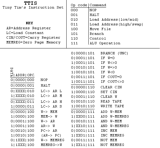
Before the design can get much further, an instruction set has to be devised. The rest of the hardware can then be designed around it. I decided to use 8 bit instructions, as it only takes up one word of memory. This will be split, as with TIM 8, into a 4 bit address with a 4 bit instruction. However as there are only 8 commands, I plan to use one of those 4 bits as a data bit. Essentially this is used to select between two alternatives in a command. It is not a particularly neat way of dealing with it, and I may change at some point. Also, the 4 bit address may make programming interesting as you have to be able to load a 12 bit address. To do this I plan to use 2 separate instructions, one utilising the data bit to switch between sections, to load the address 4 bits at a time. Again not very neat, but most of the time you will only need to change the lower 4 digits, so with careful programming it shouldn't be too much of a problem. Below is Tiny Tim's Instruction Set... or TTIS. I may think up a better, less literal name at some point, but it will do for now.
Assembler
I have started work on the assembler language, which I plan to call 'T-' . It's unlikely to be anything much more complicated than T++ , but will probably be more similar to C in it's syntax as I have started learning C/C++ and it has a very neat layout. Will post more detail in the future.
Sequencer
The sequencer controls what the computer does for each instruction. At the heart of the sequencer is a finite state machine, which generates a set of timing pulses. It outputs 5 separate signals over a period of 2 clock pulses. These signals are shown on the diagram below:
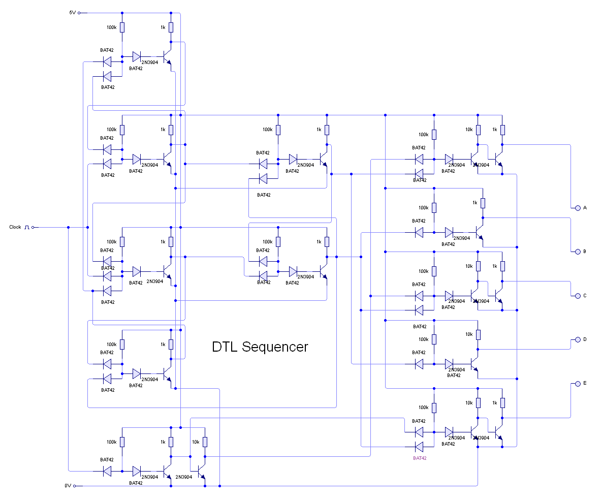
I realise there is a double inverter in there, but this is to adjust the timing so the signals come out clean. It was originally going to have 15 outputs provided by a 3 bit counter, however I quickly realised that this was far more than was needed and simplified it down to the circuit above. It is all implemented in NAND or NOT logic as they operate much faster than OR gates. Since this is the only part directly connected to the clock, it has to run faster and more precisely than any other part of the computer. It reliably clocks up to about 1 MHz on the simulator, but it's hard to tell how well it will work until I have actually built it.
The output of the FSM then goes into a set of logic that is controlled by the instruction register. This will send the timing pulses to the parts of the computer needed to execute the instruction. To illustrate what I mean, I have drawn out the timing diagram for each command.

The first two signals get the instruction from memory. This is the same for every cycle and is hardwired in. The next signal will increment the P.C. unless it is a branch instruction, in which case it will load the address register to the P.C.. The next two signals carry out the command in the instruction register. Each instruction therefore takes two clock cycles to execute.
Control Logic
This is the part of the computer that takes the instruction in the instruction register and uses it to control the rest of the machine. This is also one of the parts of the computer that is currentlty holding up construction as I failed to put much work into it's design during the original stages of this project, so it is currently badly under developed. I am currently working hard to rectify this.
It will largely consist of multiplexers, which will be used to direct the sequencer signals to the correct area of the computer. The hard part is trying to work out how to layout the instruction set in a way that will use these multiplexers most efficiently.