Prototyping and Testing
Prototype 1
Up to this point, all my circuits had been tested on a simulator (apart from that one small NOT gate right at the start), however I really needed to buy some actual components and see how well it worked in real life. I also needed to test out the components themselves to see if they were suitable. So I ordered a small batch of each type of component needed, then built a quick prototype NAND gate to check that the components at least worked together. So far so good.
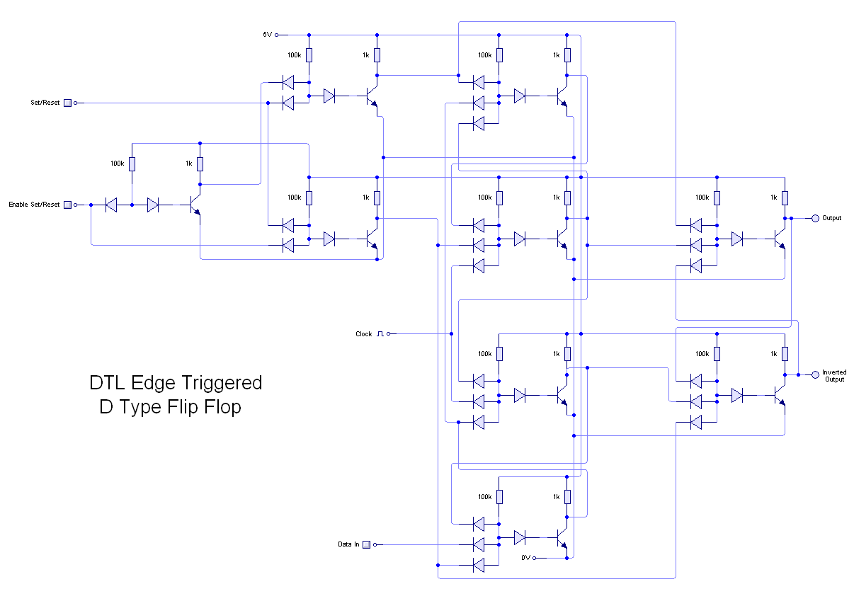
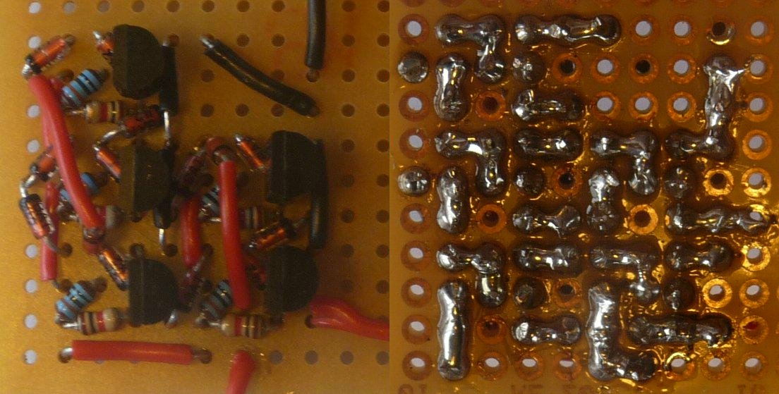
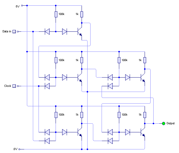
Next, I built a flip flop from this circuit diagram to work out a good layout, check that the gates worked together as expected, and to check the accuracy of my simulator. It also helped me work out a system to make construction easier.
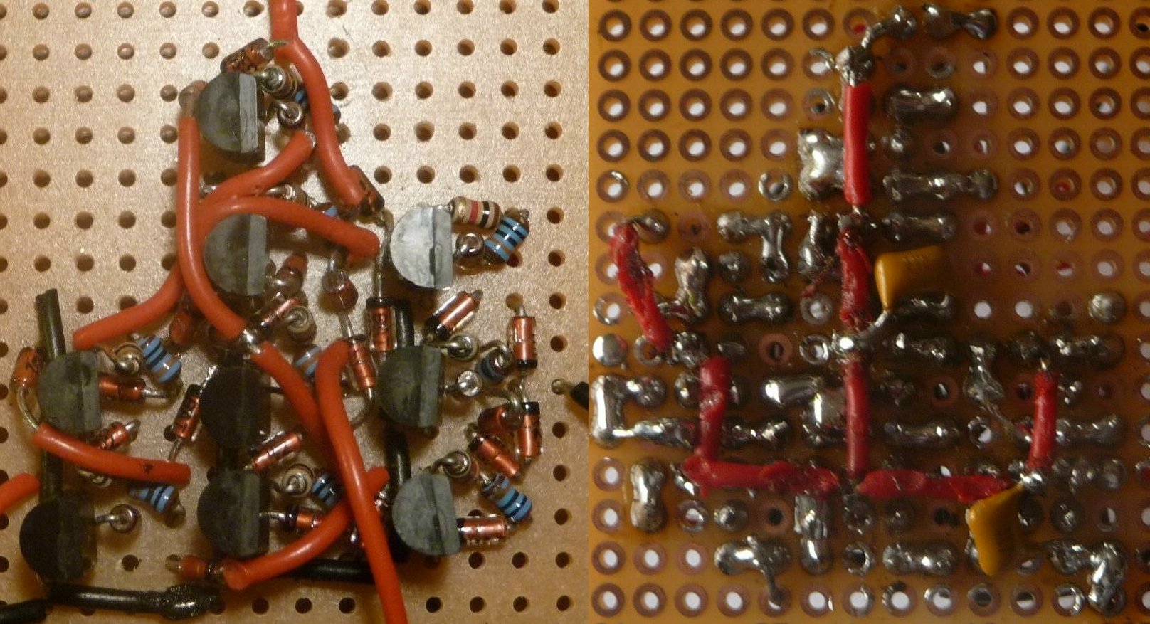
From start to finish this small circuit took me an entire day to layout, solder up and debug. A picture of the finished circuit is shown below.
The 'inverted output' was wired to 'data in', making a frequency divider which made testing easier.
The layout was alright but a bit tricky to follow as I didn't have any set format for each gate at this point. The power lines underneath were really bad though, I plan to put them on top of the board in any of my later circuits.
Testing
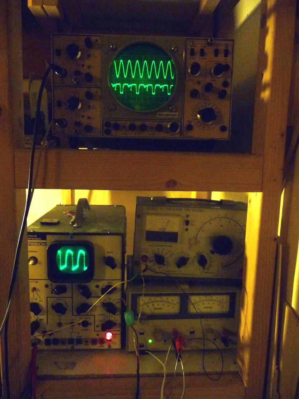
All my test equipment is fairly old and was either donated or found in the attic. (The oscilloscope on the top shelf uses valve logic)
The simulator I use for testing all my circuits before I build them is Circuit Wizard, which I got given as part of my A level electronics course. Although it is designed for basic educational purposes, I found with a bit of tweaking it can be used for simulating some pretty complex circuits at quite a high level of precision.
On first power up, I ended up with a transistor shaped burn on one of my fingers. This was due to one of the diode's being wired to the wrong place. So I moved the diode (and replaced the transistor) and tried again. This time it worked, but was occasionally missing a beat. I tried adding some capacitors to the power supply line to smooth the supply, but that didn't help. In the end it turned out that the inverted output was changing state before the edge trigger could latch properly (the problem happens to be shown on the lower trace of the top oscilloscope in the photo above) so I added a resistor between the 'inverted output' and the 'data in'. This created a basic RC circuit using the diode on 'data in' as a small capacitor, which delayed the signal enough to allow the system to latch properly.
When I'm designing a circuit on the computer, I ensure it works well up to 1 MHz. I don't expect Tiny Tim to run at this speed, but if I design all the circuits to work at 1 MHz individually, then the computer should hopefully run reliably around 200 KHz or so. To test the accuracy of the simulator, I tried running the circuit at 1 MHz, however it couldn't cope, so I turned down the frequency until it ran smoothly, which was at about 200 KHz. The results are shown below (the top trace on each is the clock pulse):
: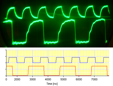
The simulator is running at 1 MHz in this example, which appears to be roughly equivalent in propogation delay to 200 KHz in reality. The circuit has quite a slow saturation period, but this is mostly due to the capacitance in the oscilloscope leads, so it's not an entirely fair test. I would repeat the test now I've found some lower capacitance leads, but unfortunately my main oscilloscope blew up spectacularly shortly after this test (I could repair it, but it would take ages and would probably blow up again, It's just too old to be reliable).
Here is a video of the circuit operating
The tests showed that the prototype did work after some adjustments, although I may improve the layout slightly in the final version. It also showed that DTL using these components was much slower than expected, so from now on I'll be assuming that 1 MHz in the simulation is roughly equivalent to 200 KHz in hardware.
Prototype 2
The components for the main build had mostly arrived by now, but I still wasn't happy with the layout. So another prototype was in order. I decided to build a basic clocked R-S flip flop, as they make up a large proportion of the circuitry, but are reasonably simple (Diagram shown here).
I started by working out a versatile layout for NAND/NOT gates (It's the same since NOT gates are just one input NAND gates in DTL). I had some new rules:
Below is the basic layout I came up with without any input diodes fitted:

(Yellow lines are 1K resistors, blue lines are 100K)
Having a standard layout means I can go through and layout the basics for each gate before I worry about any of the interconnecting logic.
Below is the circuit I came up with. Took me about an hour to build and get working (it worked first time!)
It was far easier to construct than the first prototype, and much neater. I haven't done much in the way of high speed testing yet, but I did check it would switch state at 200 KHz.
More prototypes
Having completed the flip flop above, I realised I needed far more prototypes than I originally thought. So I have since prototyped an EXOR gate and the System Clock, and have started work on a full adder. The need for these prototypes is to work out the board layout for each sub system so that board space can be optimized. I will at some point have to draw the line or I will end up prototypeing the entire computer, but for now I am still mainly focused on the design.