Logic Systems and Data Storage
Flip Flops
Once the designs for the basic gates were established, I started looking into more complicated logic systems such as flip flops and counters. The hard part here was to find circuits that used the least number of gates, whilst still performing correctly using DTL. I've gone for mostly NAND logic, as it uses the least components and has the best performance when implemented in DTL.
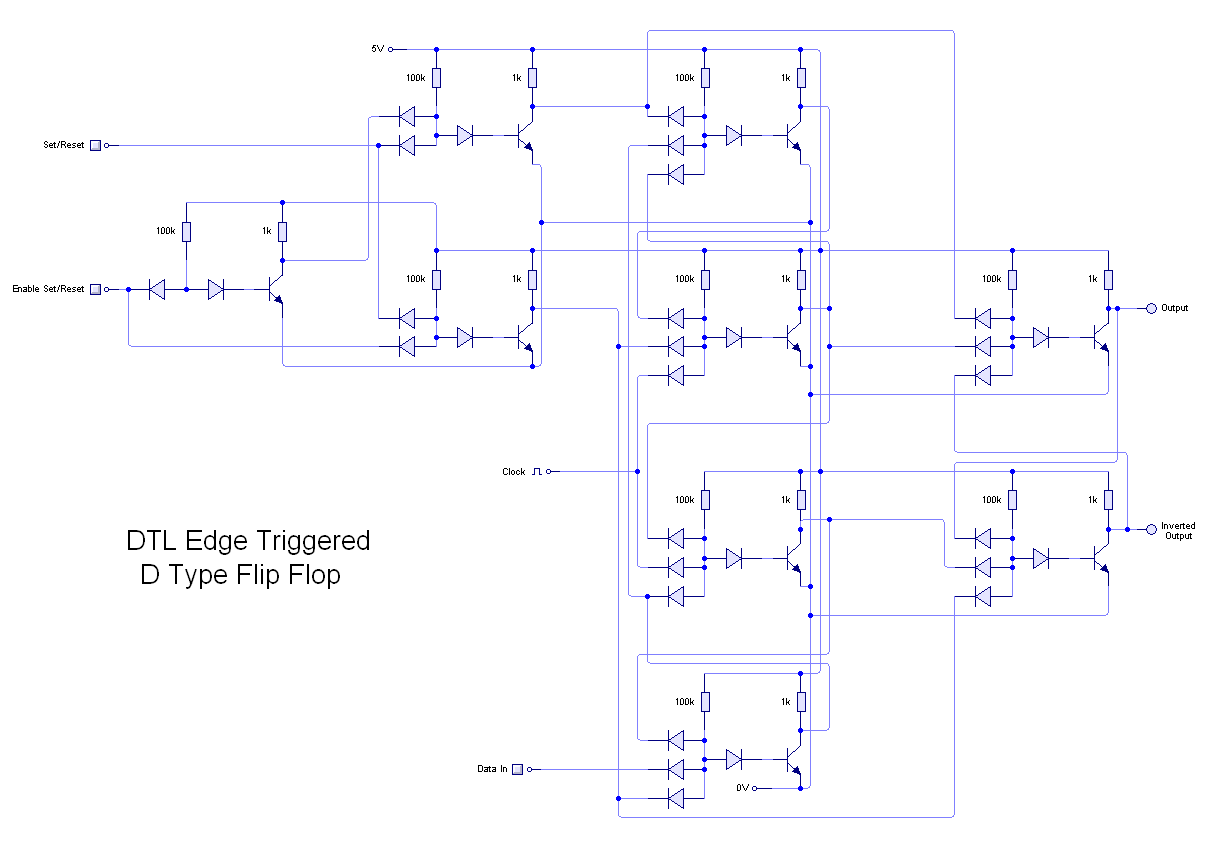
Below is an edge triggered flip flops, used for storing data:
Counters
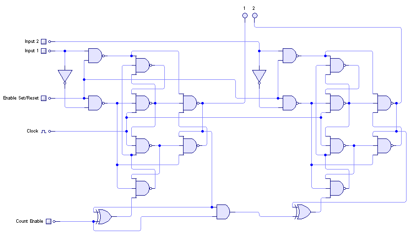
These can then be linked together to make a counter. I decided to use a synchronous counter for the program counter. Synchronous counters use a few more gates then the simpler asynchronous counters, but they are a lot faster. The set/ reset function on each flip flop allows you to insert a number into the counter, from which it can then count from. The layout for a 2 bit counter is shown below:
The program counter is a 12 bit counter, so you can imagine how many components are going to be required just for that. Once the counter design was completed, I suddenly got a sense of the shear scale of this project. But seeing as I've just started my gap year, I shouldn't be short of time!
Registers
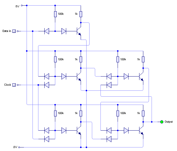
For this project I am trying to keep the number of registers to a minimum as they take up a lot of components. So far I plan to have 4 physical registers; a Working Register, an Address Register, an Instruction Register, and the Program Counter, which is basically a self incrementing register. These will all be constructed from flip flops, but different registers will use different types of flip flop. The program counter and the Working Register will be made from edge triggered D type flip flops, while the address register and working register will be made from the simpler clocked R-S flip flops (shown below). The edge triggered flip flops are needed because they are being read from and written to simultaneously, so the edge trigger makes sure it does not get stuck in a loop
. 
From now on, the Working Register is going to be referred to as the W register, and the program counter will be shortened to P.C. The other register names may well be shortened in places, but this should be obvious enough.
Memory
I have decided to use a RAM chip for this project. Yes, I don't feel great about it, but for a stored program computer it's necessary if you want to be able to achieve anything useful. Also, it's not as bad as using one on a relay computer, as at least this computer is transistor based. The chip I'm planning to use at the moment is an 8 Kilobyte SRAM chip, of which I'm only going to use one half at a time. This gives a 12 bit address, which is not so big as to make the addressing hardware huge, but is not too small so that the computer is useless. I plan to add something to switch between the top and bottom half's of the memory, so you can store two programs on there at any one time.
Zero Page Registers
To add flexibility to the computer without adding many extra components, I plan to use the first 16 bytes of zero page memory as registers that can be addressed directly with out using the address register. This allows for memory locations to remain in the address register while arithmetic fuctions take place, or for memory addresses to be stored in memory. This is nessasary as addresses have to be stored in two halves, so you can't write an address from the address register to a memory location whilst having address in the memory location. Unfortunately, ALU operations will only be possible on the first 4 of these 'registers', due to the layout of the instruction set which is detailed on the next page.