Basic Logic
Gates
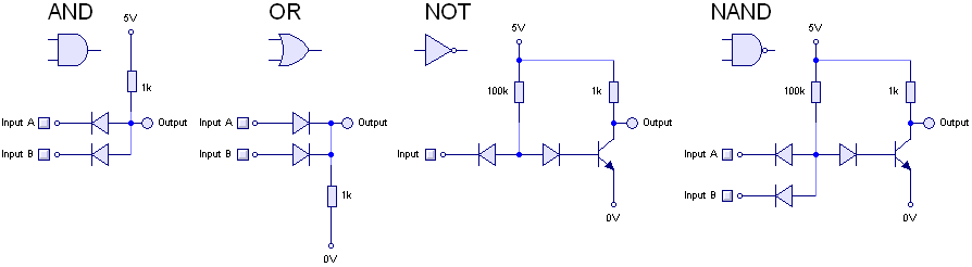
I started, as with any of my projects, by scouring the Internet for information. I quickly discovered why DTL was not a commonly used system; it is complicated, large, slow, and the wiring is a nightmare. Undeterred, I continued my research (If I could handle TIM 8's wiring, then I'm sure I can handle this, and it can't really be any larger or slower than TIM 8!). I started by looking at different designs for logic gates. I discovered that DTL logic usually consists of a combination of diode AND gates, diode OR gates, and transistor NOT gates. All other logic can be constructed out of these three gates. The diagram below should give you an idea of what I mean:
Another problem with DTL is that it that the AND and OR gates are non-regenerative; that is they have a voltage drop across them which when linked together can cause the voltage to fall significantly and create errors. For this reason I'm planning to use mainly NAND logic, as DTL inverters do regenerate the signal.
As with TIM 8, simplification is going to be key. This time it's not about cost; 500 transistors only cost a few pounds. It's more because the computer would be unnecessarily large, and would take more time to construct. Also, since building TIM 8, I have cultivated a natural urge to simplify any circuit to it's absolute basics!
To reduce the size, I've came up with standard board layouts for each gate which uses the minimum number of holes in the board. Some examples are shown below (the layout has since been improved, but this still gives you the rough idea):
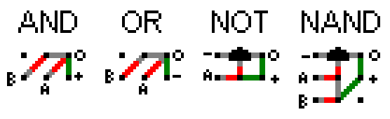
The green lines are resistors, the red lines are diodes, and the gray lines are solder links under the board. Each black square is a hole in the board. As a general rule, you can't fit more than 3 legs per hole. I also try and keep components going diagonally where possible as they can lie flat, where as the components going between two adjacent holes have too much exposed wire.
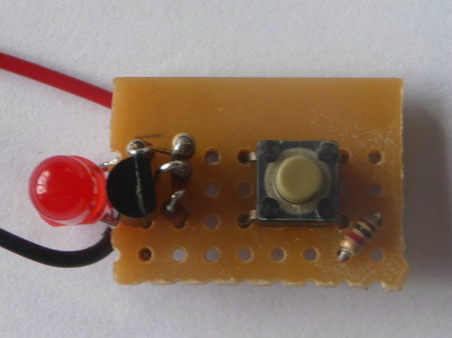
Below is my first prototype NOT gate. The gate itself takes up the 6 holes on the left hand side, the rest is just there to test that it works. It is quite fiddly to put together, and there is a risk of the exposed wires touching, so this design may be reviewed slightly, but it works fine as it is.
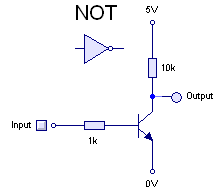
Unfortunately, my original design of inverter (shown below) had a lower component count and seemed to work fine. However SV3ORA had the official DTL inverter type on his page, which originally I couldn't see the advantage of as my version used less components and appeared to do the same thing. But when run at high speed with an oscilloscope, my inverter had a much longer delay which would mean the computer would run much slower. As one of my design criteria was speed, I changed the inverter design to the official layout as seen in the first diagram.
Most of the diagrams on these next few pages are shown with standard logic gates. That's because the DTL equivalent is quite a lot larger and would not fit on the page as well. However if you click on the pictures it will bring up the full circuit diagram for that system (If one exists).
EXOR
EXOR gates are causing a bit of a problem, as they take a large amount of components if implemented in NAND logic, but it is difficult to find a simpler circuit. As Tiny Tim uses a lot of EXOR gates (in counters, adders. etc) it is important to get the design of these gates right. After much work with the simulator and searching the internet I've decided to use this:

Although this works, It is a non-regenerative gate, so they can't be too many strung in series or the voltage will drop too low. This may be a problem in the adder, as 2 EXOR gates are stung together in each full adder. A prototype is being developed to help verify this issue.